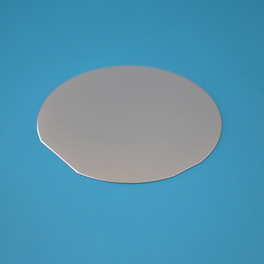
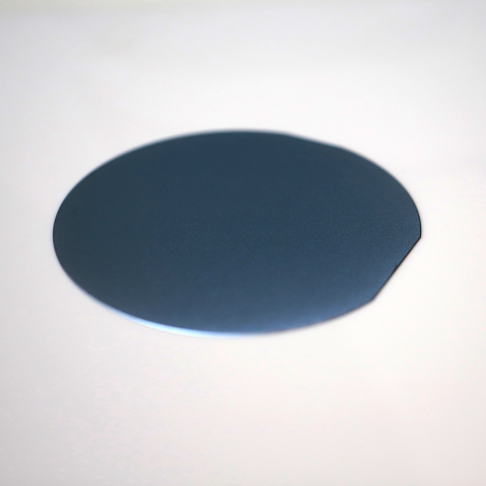
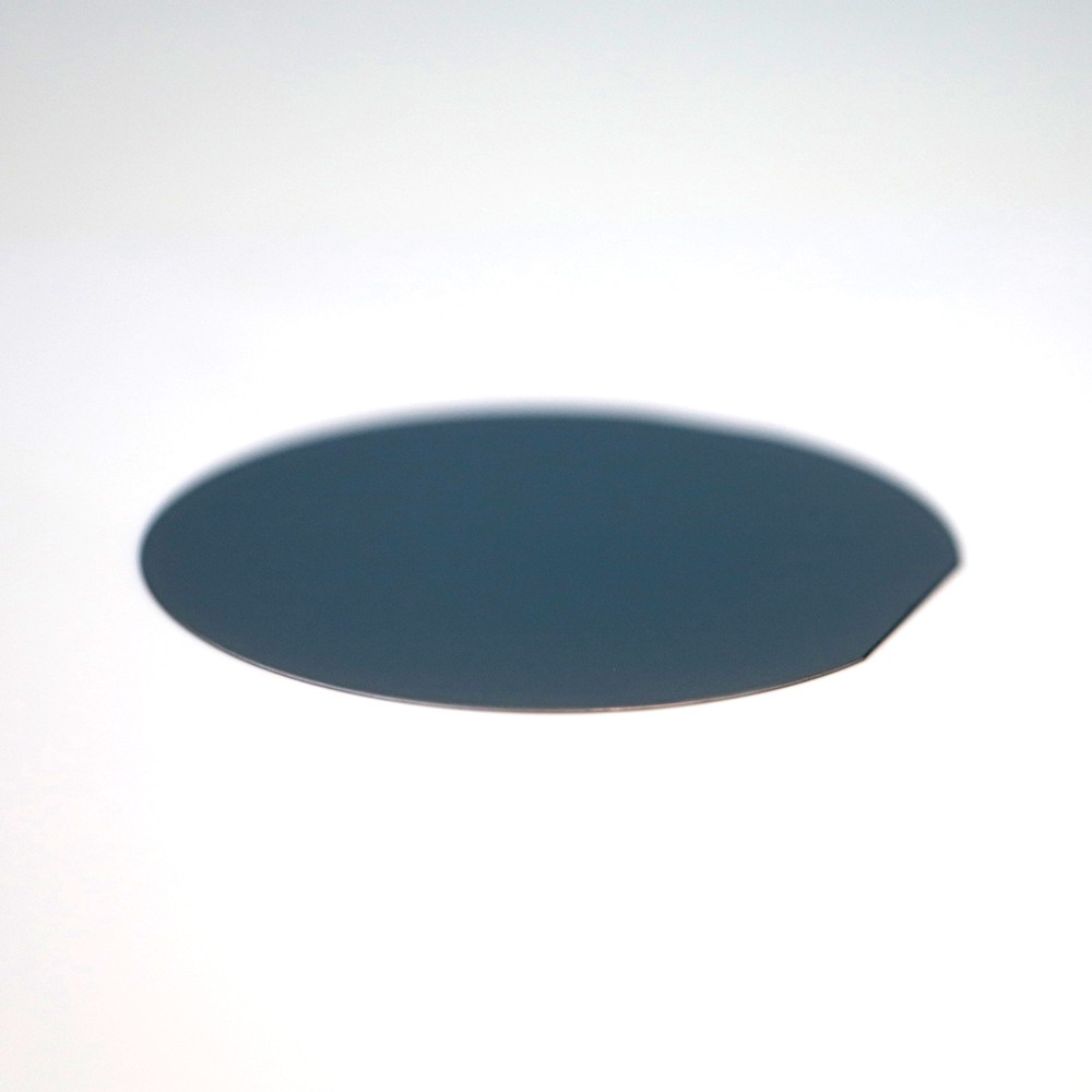
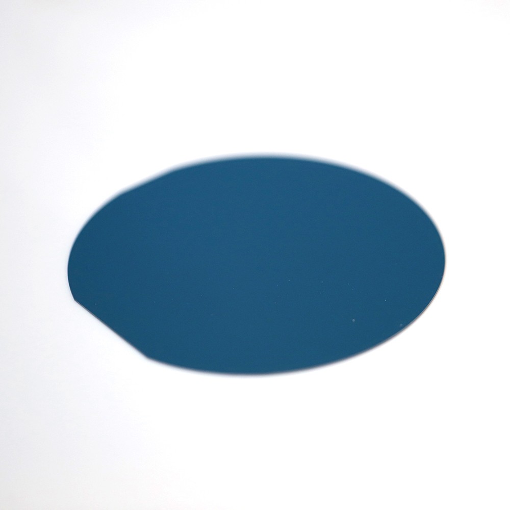
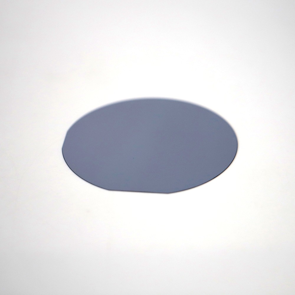
4-Inch Silicon Wafer – 100mm Prime Grade, P/N Type, <100>/<111>
Applications:
Basic Specifications:
Diameter: 100 mm (±0.2 mm, SEMI M1.2 compliant)
Thickness: 525 µm ±25 µm (standard) | 500–550 µm (custom window)
Orientation:<100> ±0.5° (most common) | <111> ±0.5° | <110> on request
Dopant / Type : P-type Boron, 1–10 Ω·cm | N-type Phosphorus, 1–5 Ω·cm
High-Resistivity : FZ, >1,000–10,000 Ω·cm (IR / sensor grade)
Surface Finish: SSP (single-side polished) | DSP (double-side polished)
TTV (Total Thickness Var) < 10 µm (standard) | < 5 µm (precision grade)
Bow : < 30 µm (standard) | < 15 µm (precision)
Warp: < 40 µm (standard) | < 20 µm (precision)
Surface Roughness:. Ra < 0.5 nm on polished face
Oxide Option: Bare | Thermal SiO₂ 100 nm – 2 µm (wet or dry)
Epitaxy Option : Epi-Si layer 1–50 µm on substrate (custom)
Cleanliness: RCA-1 + RCA-2, particle < 50 @ >0.3 µm
Packaging: 25-wafer cassette (standard) | individual anti-static sealed bag (single-wafer orders)
Material Purity: 4N (99.99%) standard | 5N / 6N on request
Flat / Notch :Primary flat: 32.5 mm (SEMI) | Notch option available